Atom Thin 2D Metals
Metals That Barely Have Thickness
Graphene taught us that materials can live as single-atom sheets and still do extraordinary things. For years, though, true metals mostly sat on the sidelines of that two-dimensional party. Layered crystals that peel apart like filo dough were easy enough to thin; ordinary metals, held together by metallic bonds in every direction, kept refusing to stretch into large, clean, atom-thin films.
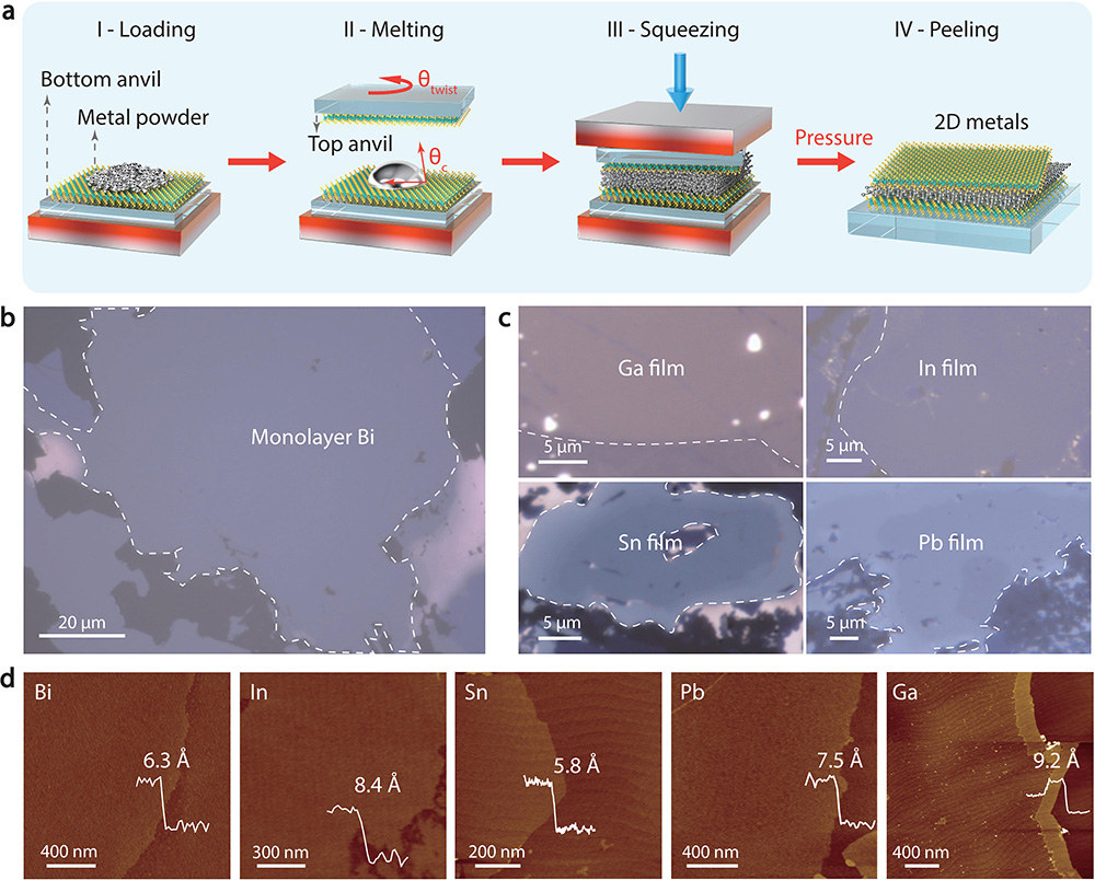
A team at the Institute of Physics of the Chinese Academy of Sciences has now coaxed several everyday metals into that extreme flatness. Their recipe is almost disarmingly physical: melt a pure metal droplet, then squeeze it hard between two specially prepared crystal surfaces until it spreads into a sheet only ångströms thick—so thin that a stack of ten would still be thinner than a typical virus.
Anvils Made of a Single Atomic Carpet
The secret is the press itself. Each “anvil” is a sapphire wafer coated with a single layer of molybdenum disulfide (MoS₂)—a smooth, dangling-bond-free carpet of atoms grown so perfectly that nothing sticks out to snag the metal. Because both sapphire and monolayer MoS₂ are extraordinarily stiff (Young’s modulus above 300 gigapascals, stiffer than many steels), they can take roughly 200 megapascals of pressure without crumpling. Under that load the molten metal is forced outward into a uniform film; when the sandwich cools, the metal freezes in place, fully sealed between the two MoS₂ sheets.
The result is not a theoretical sketch but real, peelable pieces of two-dimensional metal. Bismuth arrives at about 6.3 ångströms, tin at 5.8, lead at 7.5, indium at 8.4, and gallium at 9.2. Those numbers sit at the practical thickness limit for these elements—essentially one or a few atomic layers across macroscopic areas.
Encapsulation is more than packaging. The MoS₂ lids keep air and moisture away, so the films stay pristine long enough for careful electrical tests. Because the interfaces are non-bonded (the metal and the MoS₂ touch but do not chemically fuse), researchers can also lift the stack and build simple devices without destroying the metal’s native character.
What the Thinnest Bismuth Reveals
When the team probed monolayer bismuth, the metal behaved unlike its bulk cousin. Electrical conductivity rose sharply. Applying a gate voltage produced a clear field effect with p-type behavior—holes, not electrons, carrying the current. Spectroscopic measurements turned up large nonlinear Hall conductivity and phonon modes never seen in thicker samples. In plain language: electrons inside these ultra-flat sheets move and scatter in ways that only become visible once the third dimension is almost gone.
Pressure itself becomes a thickness dial. Dial the squeeze up or down and the same process yields monolayer, bilayer, or trilayer metal with atomic precision. That control finally lets physicists watch properties change layer by layer—an experiment that was previously out of reach for true metals.
A Workshop, Not a One-Off Trick
Corresponding author Professor Zhang Guangyu notes that the same van der Waals squeezing approach should work for metal alloys, amorphous films, and other non-layered compounds that have never been two-dimensional before. He describes a “bright vision” for quantum, electronic, and photonic devices that can now be imagined with these new building blocks, and he is frank that the field still has “plenty of room” to grow.
Caveats remain honest next steps rather than roadblocks. The metals demonstrated so far are a short list of low-melting elements; extending the method to higher-melting or more reactive metals will take engineering patience. Device work is still early—proof that intrinsic transport can be measured, not yet a catalog of finished chips. Yet each limitation points forward: thicker process windows, alloy recipes, and circuit architectures that simply could not be tried until large, stable, ångström-scale metal sheets existed.
Why the Squeeze Feels Hopeful
For two decades the two-dimensional materials story has largely belonged to crystals that already preferred to be flat. Metals were the missing chapter—the conductors we already know how to wire, solder, and pattern, now available in a form thin enough to rewrite their quantum rules. By turning a press and two perfect crystal faces into an atomic-scale rolling mill, the IOP team has handed the community a practical way to write that chapter.
The next experiments will ask how these sheets carry spin, host unusual Hall responses, or couple to light when every atom is a surface atom. Whatever answers arrive, they will rest on a simple, almost tactile idea: sometimes the way to make something new is to melt the familiar and press it until there is nowhere left to go but sideways.
"This method outlines a bright vision for a broad range of emerging quantum, electronic, and photonic devices. There is plenty of room for this new research field to grow." — Professor Zhang Guangyu