Sculpted Microscopic Helices
New research suggests that shaping magnetic weyl semimetal into intricate three-dimensional helices can introduce novel electrical behaviors, potentially paving the way for advanced devices in spintronics and beyond. By combining the intrinsic properties of a magnetic Weyl semimetal with imposed chiral geometry, scientists have demonstrated a reversible diode-like effect that operates without an external magnetic field, highlighting encouraging results in mesoscale engineering.
Breaking Symmetry Through Geometry
In materials science, symmetry often dictates how electrons, spins, and charges behave. Centrosymmetric crystals—those with a balanced, mirror-like atomic arrangement—typically limit certain phenomena, such as nonreciprocal transport, where electrical resistance differs depending on the current's direction. This is akin to a one-way street for electrons, requiring broken inversion symmetry to occur.
Results indicated that traditional approaches rely on the material's natural structure or interfaces in thin films. However, the study explores an alternative: using focused ion beam (FIB) milling to sculpt bulk crystals into curvilinear shapes. This method preserves the crystal's quality while imposing asymmetry on a mesoscopic scale, roughly between atomic and everyday sizes—think of it as engineering a twist into a straight wire to alter its conductivity.
The material in focus is Co₃Sn₂S₂, a centrosymmetric magnetic Weyl semimetal known for its high electron mobility and ferromagnetic properties. Weyl semimetals feature unique electronic states where electrons behave as if they have no mass, contributing to phenomena like the anomalous Hall effect, a transverse voltage generated by magnetization without an applied field.
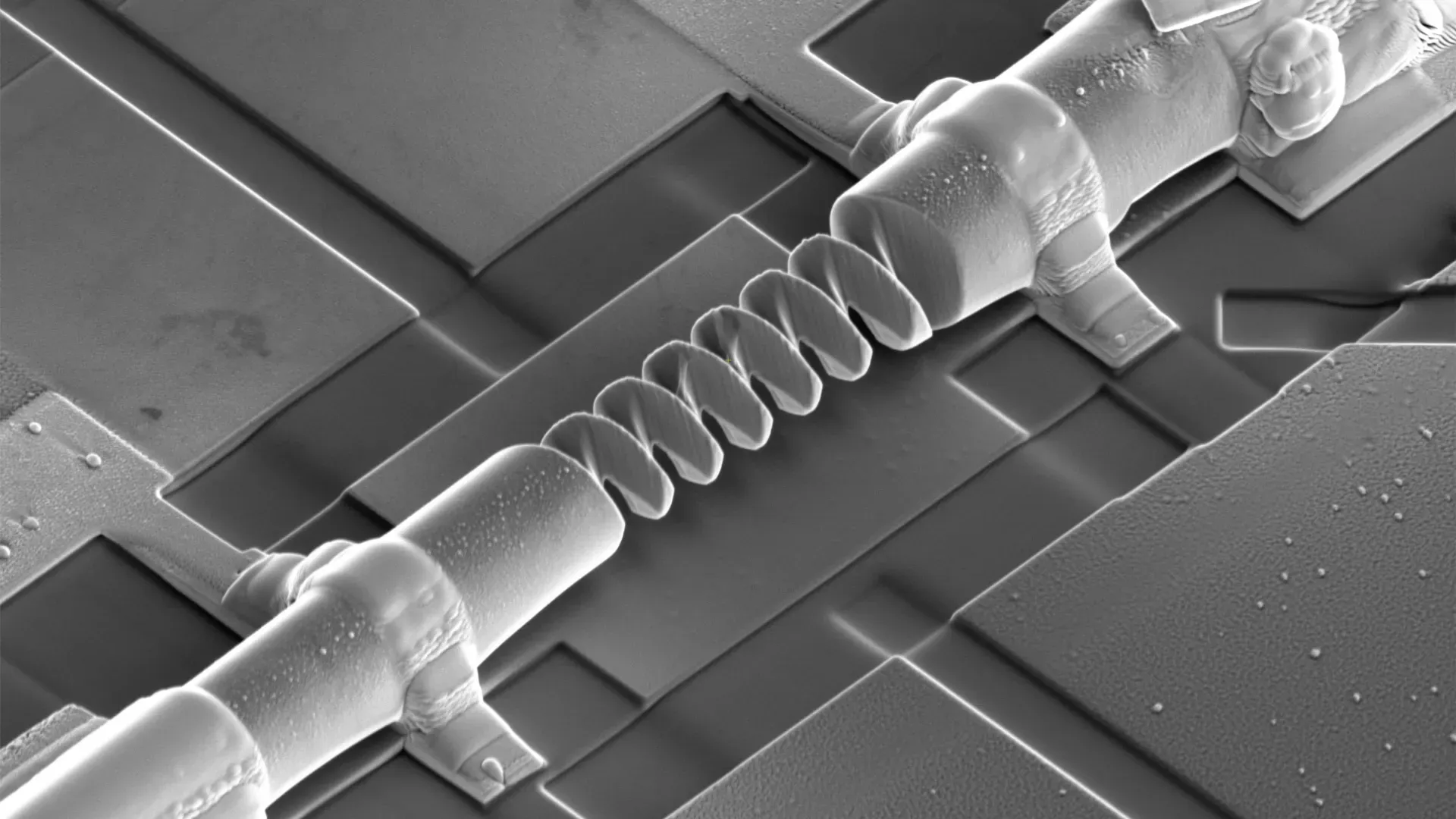
Crafting 3D Helical Devices
The methodology involved advanced FIB techniques to fabricate helical nanostructures from a single Co₃Sn₂S₂ crystal. Devices with left-handed (LH) and right-handed (RH) chirality were created, each with a pitch length around 1 micrometer—comparable to the estimated mean free path of electrons in the material, allowing quasi-ballistic transport where electrons travel with minimal scattering.
For comparison, an achiral rod-shaped device was also made. The helices were oriented along the material's magnetic easy axis, [0001], and fixed to gold electrodes on a substrate. This setup enabled precise measurements of electrical responses under varying temperatures and magnetic fields.
Transport properties were probed using AC current excitations, analyzing first and second harmonic voltages to detect nonreciprocity. The second harmonic signal, antisymmetrized to isolate the effect, revealed hysteretic behavior tied to the material's magnetization.
Revealing Anomalous Nonreciprocal Transport
Findings showed that LH and RH helices exhibit opposite signs in their nonreciprocal response, absent in the achiral device. This confirms the geometric chirality as the source. Notably, an anomalous component persists at zero magnetic field, modeled as an additional term in the voltage equation: V = R[I + (Bγ + Γ)I²], where Γ links to the intrinsic ferromagnetism.
Calculations ruled out a classical self-field mechanism—where current induces a coil-like magnetic field—as the primary cause, as the observed effect was orders of magnitude larger. Instead, results pointed to enhanced boundary scattering in the quasi-ballistic regime. As temperature drops, electron mean free paths lengthen, making device curvature crucial: asymmetrical scattering at inner and outer helix edges amplifies nonreciprocity.
Temperature-dependent data across devices with pitches of 0.5, 1.0, and 2.0 micrometers demonstrated stronger effects in smaller structures, with γ reaching 0.11 A⁻¹T⁻¹—promising when compared to other systems like bismuth helices or chiral nanotubes.
The inverse effect was also observed: applying current pulses switched the magnetization direction at 150 K, toggling the nonreciprocal signal without a field. This suggests potential for current-controlled magnetic memory.
Future Applications and Considerations
The work envisions applications in 3D spintronics, where geometry enhances quantum material functionality for high-density, low-power devices. By converging topological states with ballistic transport, it could enrich fields like magnetism and electronics.