Self Assembling Electronics
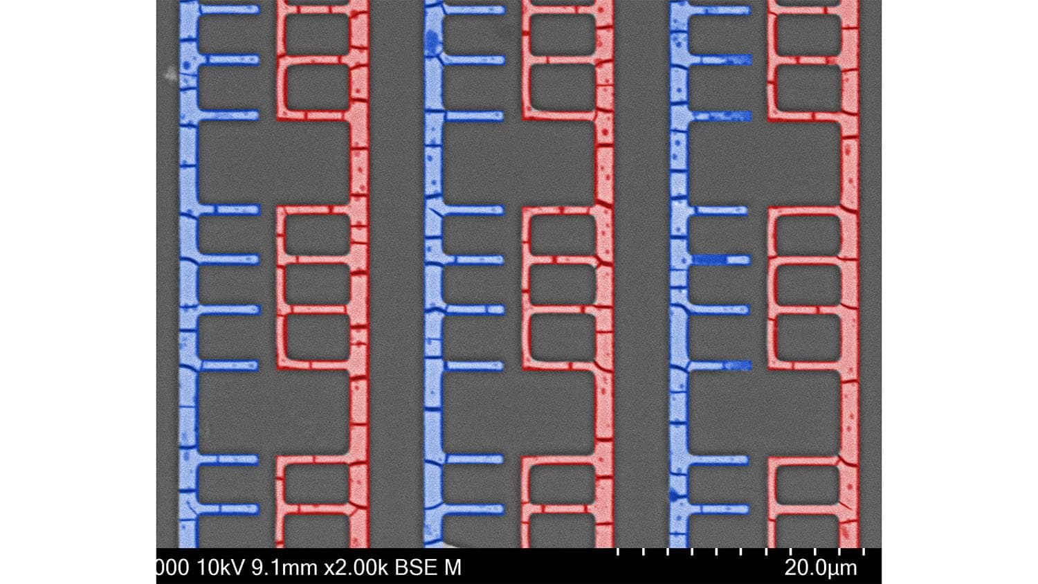
Researchers have demonstrated a new technique for self-assembling electronic devices. The proof-of-concept work was used to create diodes and transistors, and paves the way for self-assembling more complex electronic devices without relying on existing computer chip manufacturing techniques.
“Existing chip manufacturing techniques involve many steps and rely on extremely complex technologies, making the process costly and time consuming,” says Martin Thuo, corresponding author of a paper on the work and a professor of materials science and engineering at North Carolina State University. “Our self-assembling approach is significantly faster and less expensive. We’ve also demonstrated that we can use the process to tune the bandgap for semiconductor materials and to make the materials responsive to light – meaning this technique can be used to create optoelectronic devices.
“What’s more, current manufacturing techniques have low yield, meaning they produce a relatively large number of faulty chips that can’t be used. Our approach is high yield – meaning you get more consistent production of arrays and less waste.”
Thuo calls the new, self-assembling technique a directed metal-ligand (D-Met) reaction. Here’s how it works.
You start with liquid metal particles. For their proof-of-concept work, the researchers used Field’s metal, which is an alloy of indium, bismuth and tin. The liquid metal particles are placed next to a mold, which can be made to any size or pattern. A solution is then poured onto the liquid metal. The solution contains molecules called ligands that are made up of carbon and oxygen. These ligands harvest ions from the surface of the liquid metal and hold those ions in a specific geometric pattern. The solution flows across the liquid metal particles and is drawn into the mold.
As the solution flows into the mold, the ion-bearing ligands begin assembling themselves into more complex, three-dimensional structures. Meanwhile, the liquid part of the solution begins to evaporate, which serves to pack the complex structures closer and closer together into an array.
“Without the mold, these structures can form somewhat chaotic patterns,” Thuo says. “But because the solution is constrained by the mold, the structures form in predictable, symmetrical arrays.”
Once a structure has reached the desired size, the mold is removed, and the array is heated. This heat breaks up the ligands, freeing the carbon and oxygen atoms. The metal ions interact with the oxygen to form semiconductor metal oxides, while the carbon atoms form graphene sheets. These ingredients assemble themselves into a well-ordered structure consisting of semiconductor metal oxide molecules wrapped in graphene sheets. The researchers used this technique to create nanoscale and microscale transistors and diodes.
“The graphene sheets can be used to tune the bandgap of the semiconductors, making the semiconductor more or less responsive, depending on the quality of the graphene,” says Julia Chang, first author of the paper and a postdoctoral researcher at NC State.
In addition, because the researchers used bismuth in the proof-of-concept work, they were able to make structures that are photo-responsive. This allows the researchers to manipulate the properties of the semiconductors using light.

“The nature of the D-Met technique means you can make these materials on a large scale – you’re only limited by the size of the mold you use,” Thuo says. “You can also control the semiconductor structures by manipulating the type of liquid used in the solution, the dimensions of the mold, and the rate of evaporation for the solution.
“In short, we’ve shown that we can self-assemble highly structured, highly tunable electronic materials for use in functional electronic devices,” Thuo says. “This work demonstrated the creation of transistors and diodes. The next step is to use this technique to make more complex devices, such as three-dimensional chips.”
